- 您现在的位置:买卖IC网 > Sheet目录2008 > MAX1240AEPA+ (Maxim Integrated Products)IC ADC 12BIT SERIAL 8-DIP
MAX1240/MAX1241
+2.7V, Low-Power,
12-Bit Serial ADCs in 8-Pin SO
10
______________________________________________________________________________________
Using
SHDN to Reduce Supply Current
Power consumption can be reduced significantly by
shutting down the MAX1240/MAX1241 between con-
versions. Figure 6 shows a plot of average supply cur-
rent versus conversion rate. Because the MAX1241
uses an external reference voltage (assumed to be pre-
sent continuously), it “wakes up” from shutdown more
quickly (in 4s) and therefore provides lower average
supply currents. The wake-up time (tWAKE) is the time
from when SHDN is deasserted to the time when a con-
version may be initiated (Figure 5). For the MAX1240,
this time depends on the time in shutdown (Figure 7)
because the external 4.7F reference bypass capacitor
loses charge slowly during shutdown.
External Clock
The actual conversion does not require the external
clock. This allows the conversion result to be read back
at the P’s convenience at any clock rate from up to
2.1MHz. The clock duty cycle is unrestricted if each
clock phase is at least 200ns. Do not run the clock
while a conversion is in progress.
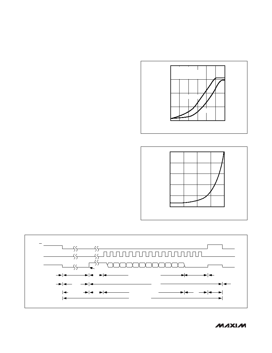
Timing and Control
Conversion-start and data-read operations are controlled
by the CS and SCLK digital inputs. The timing diagrams
of Figures 8 and 9 outline serial-interface operation.
A CS falling edge initiates a conversion sequence: the
T/H stage holds the input voltage, the ADC begins to
convert, and DOUT changes from high impedance to
logic low. SCLK must be kept low during the conver-
sion. An internal register stores the data when the con-
version is in progress.
10
1
0.01
0.001
0.1
1
10
100
1k
10k
100k
0.1
CONVERSION RATE (Hz)
SUPPLY
CURRNET
(mA)
VDD = VREF = 3.0V
RLOAD =
∞, CLOAD = 50pF
CODE = 010101010000
MAX1241
FIG.
06a
MAX1241
MAX1240
Figure 6. Average Supply Current vs. Conversion Rate
1.0
0.0
0.001
0.01
0.1
1
10
0.8
0.6
0.4
0.2
TIME IN SHUTDOWN (sec)
POWER-UP
DELAY
(ms)
MAX1240/41-07a
Figure 7. Typical Reference Power-Up Delay vs. Time in
Shutdown
EOC
INTERFACE IDLE
CONVERSION
IN PROGRESS
EOC
0
μs
TRAILING
ZEROS
IDLE
CLOCK OUT SERIAL DATA
TRACK/HOLD
STATE
TRACK
HOLD
TRACK
DOUT
B11 B10
B9
B8
B7
B6
B5
B4
B3
B2
B1
B0
SCLK
14
8
12
16
7.5
μs (tCONV)
HOLD
0
μs
(tCS)
TOTAL = 13.7
μs
12.5
× 0.476μs = 5.95μs
CYCLE TIME
CS
0.24
μs
Figure 8. Interface Timing Sequence
发布紧急采购,3分钟左右您将得到回复。
相关PDF资料
MAX1245BCPP
IC ADC SRL 12BIT 2.375V 20-DIP
MAX1249AEPE+
IC ADC 10BIT SERIAL 16-DIP
MAX1279AETC+
IC ADC 12BIT 1.5MSPS 12-TQFN
MAX1285BESA+T
IC ADC 12BIT 300KSPS 8-SOIC
MAX1302BEUG+
IC ADC 16BIT SRL 115KSPS 24TSSOP
MAX1303BEUP+
IC ADC 16BIT MULT RANGE 20TSSOP
MAX1308ECM+T
IC ADC 12BIT 8CH 4MSPS 48LQFP
MAX1320ECM+T
IC ADC 14BIT 8CH 2MSPS 48LQFP
相关代理商/技术参数
MAX1240AESA
功能描述:模数转换器 - ADC RoHS:否 制造商:Texas Instruments 通道数量:2 结构:Sigma-Delta 转换速率:125 SPs to 8 KSPs 分辨率:24 bit 输入类型:Differential 信噪比:107 dB 接口类型:SPI 工作电源电压:1.7 V to 3.6 V, 2.7 V to 5.25 V 最大工作温度:+ 85 C 安装风格:SMD/SMT 封装 / 箱体:VQFN-32
MAX1240AESA/V+
功能描述:模数转换器 - ADC 12-Bit 73ksps 3.6V Precision ADC RoHS:否 制造商:Texas Instruments 通道数量:2 结构:Sigma-Delta 转换速率:125 SPs to 8 KSPs 分辨率:24 bit 输入类型:Differential 信噪比:107 dB 接口类型:SPI 工作电源电压:1.7 V to 3.6 V, 2.7 V to 5.25 V 最大工作温度:+ 85 C 安装风格:SMD/SMT 封装 / 箱体:VQFN-32
MAX1240AESA/V+T
功能描述:模数转换器 - ADC 12-Bit 73ksps 3.6V Precision ADC RoHS:否 制造商:Texas Instruments 通道数量:2 结构:Sigma-Delta 转换速率:125 SPs to 8 KSPs 分辨率:24 bit 输入类型:Differential 信噪比:107 dB 接口类型:SPI 工作电源电压:1.7 V to 3.6 V, 2.7 V to 5.25 V 最大工作温度:+ 85 C 安装风格:SMD/SMT 封装 / 箱体:VQFN-32
MAX1240AESA+
功能描述:模数转换器 - ADC 12-Bit 73ksps 3.6V Precision ADC RoHS:否 制造商:Texas Instruments 通道数量:2 结构:Sigma-Delta 转换速率:125 SPs to 8 KSPs 分辨率:24 bit 输入类型:Differential 信噪比:107 dB 接口类型:SPI 工作电源电压:1.7 V to 3.6 V, 2.7 V to 5.25 V 最大工作温度:+ 85 C 安装风格:SMD/SMT 封装 / 箱体:VQFN-32
MAX1240AESA+T
功能描述:模数转换器 - ADC 12-Bit 73ksps 3.6V Precision ADC RoHS:否 制造商:Texas Instruments 通道数量:2 结构:Sigma-Delta 转换速率:125 SPs to 8 KSPs 分辨率:24 bit 输入类型:Differential 信噪比:107 dB 接口类型:SPI 工作电源电压:1.7 V to 3.6 V, 2.7 V to 5.25 V 最大工作温度:+ 85 C 安装风格:SMD/SMT 封装 / 箱体:VQFN-32
MAX1240AESA-T
功能描述:模数转换器 - ADC RoHS:否 制造商:Texas Instruments 通道数量:2 结构:Sigma-Delta 转换速率:125 SPs to 8 KSPs 分辨率:24 bit 输入类型:Differential 信噪比:107 dB 接口类型:SPI 工作电源电压:1.7 V to 3.6 V, 2.7 V to 5.25 V 最大工作温度:+ 85 C 安装风格:SMD/SMT 封装 / 箱体:VQFN-32
MAX1240AMJA
功能描述:模数转换器 - ADC
RoHS:否 制造商:Texas Instruments 通道数量:2 结构:Sigma-Delta 转换速率:125 SPs to 8 KSPs 分辨率:24 bit 输入类型:Differential 信噪比:107 dB 接口类型:SPI 工作电源电压:1.7 V to 3.6 V, 2.7 V to 5.25 V 最大工作温度:+ 85 C 安装风格:SMD/SMT 封装 / 箱体:VQFN-32
MAX1240BCPA
功能描述:模数转换器 - ADC Integrated Circuits (ICs) RoHS:否 制造商:Texas Instruments 通道数量:2 结构:Sigma-Delta 转换速率:125 SPs to 8 KSPs 分辨率:24 bit 输入类型:Differential 信噪比:107 dB 接口类型:SPI 工作电源电压:1.7 V to 3.6 V, 2.7 V to 5.25 V 最大工作温度:+ 85 C 安装风格:SMD/SMT 封装 / 箱体:VQFN-32